
This application note presents a methodology for modeling and designing a wideband 2–6 GHz local-oscillator (LO) driver amplifier with the objective of minimizing additive phase noise (APN). The initial design process relies on the standard device-level data required for conventional driver-amplifier development, including S-parameters, noise figure, output-power compression, and saturated-output-power performance over the intended operating frequency range.
For LO driver applications in which APN is a critical performance metric, conventional RF characterization is necessary but not sufficient. Each candidate active device should also be characterized for amplitude-modulation-to-phase-modulation (AM-to-PM) distortion and APN behavior as functions of both input drive level and carrier frequency.
APN measurements taken at a single input-power level or carrier frequency provide only a limited representation of device behavior. A more complete assessment should sweep the device from small-signal operation through gain compression and into saturation, since LO driver amplifiers are commonly biased and driven near these operating regions.
As an active device transitions into compression and saturation, AM-to-PM distortion can increase and materially degrade APN performance. This relationship is especially relevant for LO driver amplifiers because the desired operating point may coincide with the onset of nonlinear phase conversion.
AM-to-PM behavior is strongly dependent on active device topology, bias condition, output loading, and carrier frequency; therefore, it should not be inferred from nominal gain-compression or output-power data alone. In the absence of broadly accepted predictive rules for AM-to-PM performance under compressed operation, each candidate amplifier should be measured directly and evaluated under conditions representative of the intended application.
To support device selection and low-APN design optimization, AM-to-PM measurements should be acquired in parallel with the standard RF characterization data set, including:
Modern vector network analyzers make AM-to-PM characterization practical to integrate into the device-evaluation workflow. When direct APN measurements are unavailable or limited in scope, AM-to-PM data provides a valuable alternative for assessing how phase-noise performance may vary with input drive level, compression state, and carrier frequency.
The following example illustrates the application of the proposed design methodology to a wideband LO driver amplifier. The design target is defined by the specifications summarized below.

A preliminary review of these requirements indicates that a two-stage cascade of InGaP/GaAs heterojunction bipolar transistor (HBT) amplifiers, combined with gain-slope equalization, is an appropriate starting topology. The Mini-Circuits GALI-39+ is considered as a candidate for the first stage, while the GVA-83+ is considered as a candidate for the second stage.
To evaluate their suitability, each amplifier was modeled in Keysight ADS using the Amplifier2 behavioral model. This model requires an MDF file and a compatible ADS workspace. MDF files are available for many Mini-Circuits amplifiers and may also be requested from the Mini-Circuits Application Engineering team. Published application notes and blog posts describe the process for creating MDF files and configuring the ADS workspace. The resulting performance data for each amplifier is summarized in the following sections.
GALI-39+


The GALI-39+ exhibits favorable small-signal performance over the 2–6 GHz operating range; however, its available output power is insufficient to directly support mixer and multiplier LO-port drive levels of +18 dBm. In addition, the device exhibits an approximate 3.5 dB negative gain slope across frequency, which must be addressed through gain-slope equalization in the amplifier chain.
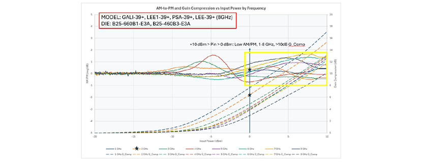
Despite these limitations, the AM-to-PM (AM/PM) and APN results shown in Figures 3 and 4 indicate that the GALI-39+ provides exceptionally strong nonlinear additive phase-noise performance. These characteristics make it a compelling candidate for use as an early-stage device in low-additive-phase-noise LO driver amplifier chains, where preserving additive phase-noise performance is a primary design objective.


The blue trace in Figure 4 represents small-signal operation and can be used to estimate the device noise figure. After accounting for the input loss of the test fixture, this result agrees closely with the noise-figure data shown in Figure 2. The best APN performance occurs at an input power of +6.4 dBm. When the device is driven at +11.3 dBm, corresponding to more than 15 dB of gain compression, APN degrades by less than 3 dB. This result indicates that the GALI-39+ maintains strong nonlinear additive phase-noise performance even under substantial compression. As expected, these results are consistent with its exceptionally strong nonlinear AM/PM performance.


The GVA-83+ also exhibits favorable small-signal performance over the 2–6 GHz operating range, and its available output power is more than sufficient to directly support mixer and multiplier LO-port drive levels of +18 dBm. However, the device does exhibit an approximate 5.5 dB negative gain slope across frequency, which must be addressed through gain-slope equalization in the amplifier chain.
Despite these limitations, the AM-to-PM and APN results shown in Figures 7 and 8 indicate that the GVA-83+ provides exceptionally strong nonlinear additive phase-noise performance. These characteristics make it an excellent candidate for use as the final output-stage device in low-additive-phase-noise LO driver amplifier chains, where preserving phase-noise performance is a primary design objective.


The green trace in Figure 8 represents an approximate small-signal operation and can be used to estimate the device noise figure. After accounting for the input loss of the test fixture and the higher than optimum input power level used, the result also agrees closely with the noise-figure data shown in Figure 5. The best APN performance occurs at an input power of +6.2 dBm. When the device is driven at +9.2 dBm, corresponding to more than 4 dB of gain compression, APN remains below -167 dBc/Hz, a key result for this design that also highlights the exceptional APN versus input power performance of the HBT based design. This result indicates that the GVA-83+ maintains strong additive phase-noise performance even under substantial compression. As expected, these results are consistent with its exceptionally strong AM/PM performance.
As an initial step in the cascaded-amplifier design, the small-signal response of the GALI-39+ and GVA-83+ was evaluated without gain-slope equalization. As shown in Figure 9, the cascaded response exhibits an approximately 8.7 dB decrease in gain across the 2–6 GHz operating band, confirming the need for interstage equalization.

To compensate for the negative gain slope, two EQY-8-63+ positive-slope equalizers were inserted between the amplifier stages. Positioning the equalizers after the low-noise GALI-39+ minimizes degradation of the cascaded noise figure. A provision for a YAT-series attenuator pad was included between the equalizers to provide fine adjustment of the drive level into the GVA-83+ output stage. This adjustment enables the GVA-83+ input power to be set within the range associated with optimum APN performance.

Figure 11 presents the combined small-signal response of the equalized LO driver amplifier. The peak-to-peak gain variation is less than 1 dB across the 2–6 GHz operating band. The equalization network only increases the cascaded noise figure by approximately 1 dB at the worst-case frequency of 2 GHz.

Although cascaded small-signal results are necessary for conventional amplifier design, they are insufficient to characterize LO driver amplifiers that typically operate in compression or saturation. The drive level applied to each amplifier stage must therefore be carefully set and controlled to achieve optimum APN performance while minimizing degradation caused by AM-to-PM distortion.
Large-signal simulations of the GALI-39+ and GVA-83+ were performed in Keysight ADS using the Amplifier2 behavioral model. Each device’s model requires a corresponding MDF file and a compatible ADS workspace. MDF files are available for many Mini-Circuits amplifiers and may also be obtained from Mini-Circuits Application Engineering. Published application notes and technical articles provide further guidance on MDF-file generation and ADS workspace configuration.
For this analysis, the carrier frequency was swept from 1 to 7 GHz, and the input power to the amplifier cascade was swept from −20 to 0 dBm. The upper limit of 0 dBm corresponds to the minimum specified synthesizer output power.
Figure 12 presents the simulated large-signal performance of the first-stage GALI-39+, with markers positioned near 2, 4, and 6 GHz.
At the minimum specified synthesizer output power of 0 dBm, the GALI-39+ operates at approximately 4 dB of gain compression and delivers approximately +12 to +15 dBm over the 2–6 GHz band. The measured data in Figure 3 shows low AM-to-PM distortion for input powers from 0 to +10 dBm. Therefore, the simulated operating point at the minimum synthesizer drive level remains within the device’s acceptable AM-to-PM operating region.

Figure 13 presents the large signal simulation results for the GALI-39+ and gain slope equalizer with markers positioned near 2, 4, and 6 GHz.

The effectiveness of equalization network on small signal response has been demonstrated by Figures 10 and 11. However, the effect on input power to the GVA-83+ and the resulting impact to APN and AM-to-PM distortion must still be determined. As shown in Figure 13, input power to the GVA-83+ is approximately +3 dBm at 2 GHz, increasing to approximately +10 dBm at 6 GHz. Compared against Figures 7 and 8, it is clear that this input power range is acceptable from both an APN and AM-to-PM perspective.
Figure 14 presents the simulated large-signal performance of the complete LO driver amplifier.

The complete amplifier exhibits approximately 7 dB of overall gain compression and a minimum output power of approximately +18.5 dBm at 6 GHz, thereby satisfying the specified output-power requirement. Although not directly apparent from Figure 14, the drive levels applied to both the GALI-39+ and GVA-83+ were adjusted to minimize APN and AM-to-PM distortion. Experimental validation of the simulated results is presented in the following section.
Figure 15 compares the measured and simulated gain and output-power responses of the GALI-39+. The close agreement between measurement and simulation validates the Amplifier2 behavioral model and the associated MDF data available from Mini-Circuits.

Figure 16 compares the measured and simulated Gain and Output Power response of the GVA-83+. As was the case for the GALI-39+, the close agreement between measurement and simulation validates the Amplifier2 behavioral model and the associated MDF data available from Mini-Circuits.

Figure 17 presents the measured AM-to-PM distortion and gain-compression characteristics of the cascaded amplifier. The results demonstrate that cascading the two amplifier stages does not materially degrade the overall AM-to-PM performance. Moreover, the cascade can be driven into saturation without a significant increase in AM-to-PM distortion, indicating that saturated operation is acceptable for the intended LO driver application.

Figure 18 presents the measured and simulated Gain and Output Power response of the cascaded LO Drive Amplifier. As was demonstrated previously, the close agreement between measurement and simulation validates the Amplifier2 behavioral model and the associated MDF and S-Parameter files available from Mini Circuits.

Figure 19 presents the measured and simulated small signal gain response of the LO Drive Amplifier. The close agreement once again confirms the validity of the Amplifer2 behavioral models and the data comprising the MDF and S-Parameter files available from Mini Circuits.

Figure 20 presents the measured additive phase noise (APN) of the LO driver amplifier at a 2 GHz carrier frequency for input powers from 0 to +5 dBm in 1 dB increments. Relative to the individual-amplifier APN measurements shown in Figures 4 and 8, the flicker-noise component at a 100 Hz offset increases by approximately 3 dB, consistent with the theoretical increase for two statistically independent amplifier stages connected in cascade. At a 10 kHz offset, the measured APN satisfies the −165 dBc/Hz requirement. Notably, the APN remains essentially constant across the 5 dB input-power range. This behavior is consistent with the AM-to-PM results in Figures 3 and 7 and demonstrates the importance of characterizing AM-to-PM distortion when establishing the acceptable drive-level range for each amplifier stage.

Figure 21 presents the measured additive phase noise (APN) of the LO driver amplifier at a 6 GHz carrier frequency for input powers from 0 to +5 dBm in 1 dB increments. At a 100 Hz offset, the measured flicker-noise component is limited by the test-equipment noise floor of approximately −146 dBc/Hz, represented by the red trace in the figure. At a 10 kHz offset, the measured APN reaches approximately −158 dBc/Hz; however, this result is also influenced by the test-equipment noise floor. Despite this measurement limitation, the APN remains essentially constant across the 5 dB input-power range. This behavior is consistent with the AM-to-PM results in Figures 3 and 7 and further demonstrates the importance of characterizing AM-to-PM distortion when establishing the acceptable drive-level range for each amplifier stage.

This application note presented a methodology for modeling and designing a wideband 2–6 GHz local-oscillator (LO) driver amplifier with the objective of minimizing additive phase noise (APN). The initial design process relied on the standard device-level data required for conventional driver-amplifier development, including S-parameters, noise figure, output-power compression, and saturated-output-power performance over the intended operating frequency range.
For LO driver applications in which APN is a critical performance metric, conventional RF characterization was shown to be necessary but not sufficient. Each active device was characterized for amplitude-modulation-to-phase-modulation (AM-to-PM) distortion and APN behavior as functions of both input drive level and carrier frequency. A complete assessment included sweeping the device from small-signal operation through gain compression and into saturation, as LO driver amplifiers are commonly biased and driven near these operating regions. The importance of characterizing AM-to-PM distortion when establishing the acceptable drive-level range for each amplifier stage has been clearly demonstrated.
Wideband 2–6 GHz LO Driver Amplifier Behavioral Modeling and Design for Minimum Additive Phase Noise
Impact of Additive Phase Noise on Frequency Multiplier Chains for SATCOM.
Cascade System Analysis Using Amplifier2 Behavioral Models in Keysight ADS.
Using S-Parameter Files to Model Small and Large Signal Amplifier Performance in Keysight ADS.
Additive Phase Noise Part 1: Understanding Additive Phase Noise in RF & Microwave Amplifiers.
Additive Phase Noise Part 2: Understanding Additive Phase Noise in RF & Microwave Amplifiers.
Additive Phase Noise Part 3: Cascaded RF Amplifier APN Performance