Anatomy of a 37-40 GHz 5G n260 Band Front-End with a Discrete LO
The appetite for greater download speeds and lower latency amongst modern mobile device users can be satisfied by higher RF bandwidths. The greatest bandwidths available are found in the mmWave bands, such as 5G band n260 (often referred to as the 39 GHz band, or upper Ka band) which spans 37 to 40 GHz. Although signals in the mmWave band region have the shortest range and poorest ability to penetrate obstacles like buildings and irregular terrain, they do afford the opportunity to achieve incredibly high data rates. Devices capable of receiving the 5G n260 band are theoretically capable of achieving download speeds of up to 20 Gbps under ideal conditions, such as over a short range (< 500 meters) and for line-of-sight transmission. Under real-world conditions, one of the major telecommunications network operators has deployed a 5G FR2 n260 band solution that offers speeds up to 3 Gbps1, and every one of the top three operators has deployed n2601, predominantly where dense wireless traffic is located – stadiums, convention centers, large urban areas, etc.
In this article we examine a 5G n260 band discrete mmWave front end/downconverter, replete with a discrete local oscillator (LO). Performance estimates over the 37 to 40 GHz RF band prove to be excellent when calculated using cascade analysis. Perhaps the most impressive aspect of this discrete solution is that each and every part of the RF, LO, and IF chains was born and bred right here at Mini-Circuits.
Front and Center – The RF Front End
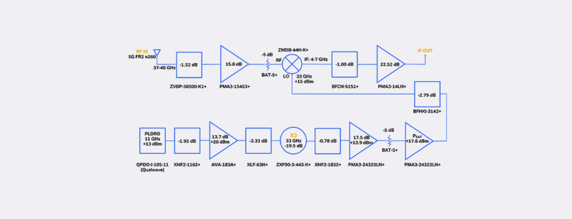
A notional front end that down-converts the 5G 37-40 GHz n260 RF band to an IF band of 4-7 GHz is shown in Figure 1. The Mini-Circuits’ ZVBP-38500-K1+ bandpass filter covering 37-40 GHz is utilized as a preselector to set the system bandwidth at 3 GHz (and consequently the noise floor to ≈-79 dBm) until downstream filtering narrows (channelizes) the 3 GHz band and reestablishes the system bandwidth and noise floor. The frequency response of the ZVBP-38500-K1+ cavity bandpass filter is shown in Figure 2. Notice how characteristically steep the skirts are. Insertion loss in the center of the band is also quite low at 1.52 dB.
The preselected 5G n260 37-40 GHz band is amplified by the PMA3-15453+ LNA, padded down by the BAT-5+ fixed attenuator and input to the ZMDB-44H-K+ for down-conversion to IF. The PMA3-15453+ LNA has a noise figure of 3.4 dB and a gain of 15.8 dB, as shown in the figure. Another excellent feature of the PMA3-15453+ is its input power handling of +23 dBm, which is well above the flat leakage of most limiters if one were to be necessary up front. The BAT-5+ improves the match seen by the LNA and mitigates reflections from the mixer. The n260 band is then down-converted as the ZMDB-44H-K+ mixer beats it against its 33 GHz LO to establish the difference frequency as the 4-7 GHz IF. The ZMDB-44H-K+ mixer requires an LO power of +15 dBm and has a conversion loss of just over 10 dB when converting 38.5 GHz to 5.5 GHz by way of a 33 GHz LO.
The output of the mixer is band-limited to 4-7 GHz at IF by the Mini-Circuits’ BFCN-5151+ LTCC bandpass filter. This filter had such optimum bandwidth for the application that it was chosen despite its reflective nature. Mini-Circuits’ reflectionless filter line is also an ideal choice when designing filters around frequency conversion components like mixers and multipliers. The PMA3-14LN+ from Mini-Circuits is utilized as the IF amplifier. With a low noise figure of just 1.25 dB and high gain of 22.52 dB at the IF band center (5.5 GHz) that remains flat across the 4-7 GHz IF band, this amplifier is a worthy choice for the IF application.


Figure 2. ZVBP-38500-K1+ cavity bandpass filter performance showing the 5G n260 passband and steep skirts
RF Front End Performance
A cascade analysis was performed on the 5G n260 band front end when converting from 37-40 GHz RF to 4-7 GHz IF. Calculations were performed every 0.5 GHz, and the tabular results of those calculations are shown in Table 1. The eyes of the receiver designers will go immediately to the IP1dB and IIP3 columns and those of the transmitter designers to the OP1dB and OIP3 columns to get a feel for the RF front end performance. Whichever way it is viewed, the RF front end is operable at a sufficiently high gain and linearity while maintaining noise figure low enough to successfully down-convert the 5G n260 frequency band. Additional figures are shown after Table 1 and illustrate relatively flat performance for gain and NF (Figure 3), IP1dB and IIP3 (Figure 4) and OP1dB and OIP3 (Figure 5) across the 3 GHz band.


Figure 5. 5G n260 RF front end cascade analysis showing OP1dB and OIP3 vs. frequency
LO and Behold – Building a 33 GHz LO
While little attention has been paid to the 33 GHz local oscillator (LO) thus far, this section takes a deeper dive into its design and electrical characteristics, and ultimately into how the LO can affect the overall RF front end system performance.
Starting Small – Low Phase Noise
5G systems are inordinately sophisticated and comprised of Orthogonal Frequency Division Multiplexing (OFDM), with the commensurate closely-spaced (60 kHz, 120 kHz) subcarriers, and often include higher-order Quadrature Amplitude Modulation (QAM) such as 256-QAM and even 1024-QAM. Why would a designer need to concern themselves with such system issues when simply building an LO? That question can be answered in two words…phase noise. Phase noise is defined as random phase fluctuations of a carrier (in our case the LO) which, in the frequency domain are spread into noise sidebands that are adjacent to the carrier. Alternatively, phase noise can be converted to rms phase jitter in the time domain. Since the LO application was for the mmWave band 5G n260, we took great care in the design to choose something reasonably low in phase noise, the Qualwave QPDO-I-105-11 phase-locked dielectric resonator oscillator (PLDRO). Based upon the manufacturer’s data, we have taken the liberty to plot the upper sideband from 100 Hz to 1 MHz offset from the 11 GHz carrier, and to compute the integrated phase noise across that range of offsets, as well as some time domain equivalent figures.
Frequency Multiplication
We utilize 11 GHz as our fundamental frequency and a Mini-Circuits’ tripler to form the 33 GHz LO due to the upper frequency limitations of dielectric resonator oscillators. We could have used an Opto-electronic oscillator (OEO) or a Gunn diode oscillator in place of our LO chain, but there’s no fun in that. However, we do pay a price for tripling the frequency insofar as the phase noise will increase:
Phase noise increases for n x f0 by 20log(n) = 20log(3) = 9.54 dB ≈ 10 dB
Consequently, our phase noise at 33 GHz will be approximately 10 dB worse than -60 dBc, or -50 dBc.

Figure 6. Phase noise sideband for the 11 GHz LO from 100 Hz to 1 MHz offset. Integrated phase noise also shown on the chart
Filtering and Multiplication – A 33 GHz LO in the Making
The bottom (LO) section of Figure 1 shows the Qualwave 11 GHz PLDRO feeding the reflectionless XHF2-1162+ high pass filter which has less than 2 dB of loss and attenuates, without reflecting any of the subharmonics that are often typical of a PLDRO. The AVA-183A+ is driven by an 11 GHz carrier at +11 dBm, driving it into saturation at approximately P5dB and yielding an output of +20 dBm. Another reflectionless filter, the XLF-63H+ low pass filter limits transmissions from the AVA-183A+ amplifier to only the 11 GHz fundamental, attenuating (and absorbing) the second harmonic by over 40 dB, and absorbing higher order harmonics as well. The excellent spectrum cleanup exhibited by the XLF-63H+ reflectionless filter comes at the price of just over 3 dB of loss. The AVA-183A+ drives the 11 GHz fundamental through the XLF-63H+ low pass filter and into the ZXF90-3-443-K+ 3X multiplier with a carrier level of approximately +17 dBm. In tripling 11 GHz to achieve our 33 GHz LO frequency, the multiplier exhibits a conversion loss of nearly 20 dB, and multiple harmonics are generated in the conversion process. While the ZXF90-3-443-K+ tripler does a great job of suppressing the fundamental (-45 dB), second (-40 dB) and fourth (-40 dB) harmonics, the XHF2-1832+ reflectionless high pass filter provides an additional 16 dB of absorptive attenuation at the fundamental frequency, a belt-and-suspenders means of cleaning up the 33 GHz LO before amplification.
LO MMIC Amplification and High-Rejection Filtering
Boosting the LO signal is handled by a pair of PMA-24323LN+ MMIC low noise amplifiers operating in Ka band. These amplifiers operate with a gain of 17.5 dB and an OP1dB of +16.6 dBm at 33 GHz. The first PMA-24323LN+ stage is operated linearly, boosting the -3.6 dBm 33 GHz signal to +13.9 dBm. While an interstage BAT-5+ attenuator pads this level down to +8.7 dBm, that is still sufficient to drive the final PMA-24323LN+ stage heavily into saturation (P9dB), yielding +17.6 dBm, an additional dB of output power beyond P1dB. Compressing the final MMIC amplifier stage by 9 dB at 33 GHz will also tend to raise the other harmonics that are not in compression. Enter Mini-Circuits’ HK-Series of SMT high-rejection filters, and in particular, the BFHKI-3142+ bandpass filter. Not only is this series tiny, but for the signals of interest, the 11 GHz fundamental is suppressed by 68 dB, the 22 GHz second harmonic by 80 dB and the fourth harmonic by 60 dB, while the desired 33 GHz LO slips by with an insertion loss of less than 3 dB. This final filtering stage ensures that the LO signal is clean and free from spurious and harmonic signal levels that might affect front end performance.
5G n260 Band System Performance
There are a multitude of parameters that can be considered when analyzing system performance, particularly for systems as sophisticated as 5G, where OFDM and QAM are common. Let’s assume that the system GNIP (Gain, NF, IP3, P1dB) is sufficient to meet the system link budget, and that the IF output level is also adequate to drive a balun and subsequently an ADC/FPGA for digital backend processing. Now, with the RF performance and IF amplitude level taken care of, and taken off the table, we’re left with perhaps one of the most crucial performance parameters in all of wireless communications today, phase noise, or phase jitter. For our system, the 33 GHz LO is the main, if not the only major contributor. Note that while MMIC amplifiers have their own additive phase noise, their performance is generally orders of magnitude better than a typical PLDRO, so we have not addressed it. Mini-Circuits does have a cadre of very low additive phase noise amplifiers and an excellent series of articles2 and videos3 discussing additive phase noise in RF and microwave amplifiers.
Getting back to the 33 GHz LO phase noise and RMS phase jitter. From the inset in Figure 6, we know that the integrated phase noise is -60 dBc and RMS phase jitter is 85 m⁰ at the 11 GHz fundamental. We previously determined that our phase noise would increase by approximately 10 dB to become -50 dBc when we triple the fundamental LO frequency to 33 GHz. To calculate the RMS phase jitter at 33 GHz, we use the equation:
New Phase JitterRMS = Old Phase JitterRMS x (10(A/20)) where A is the ratio of the new to the old integrated phase noise in dB. In our case, A is 10 dB and we have: New Phase JitterRMS = 0.085⁰RMS x (10(10/20)) = 0.269⁰RMS. To put this magnitude of RMS phase jitter into perspective, we examine Figure 7 below where several values of RMS phase jitter are plotted against bit error rate (BER) and signal-to-noise ratio (SNR). 0.269⁰RMS is sufficiently close to 0.25⁰RMS to use that curve as a reference, and using a BER of 10-9 as a reasonable benchmark for our 256-QAM system, we find that, in order to achieve a BER of 10-9 we must also have an SNR of 35 dB. While we know the mid-band NF to be 7.37 dB, and we previously calculated the noise floor for a 3 GHz system to be -79 dBm, that is not to say that our signal level must be 35 dB greater than the (-79 dBm + 7.37 dB = -71.63 dBm) noise floor to achieve a BER of 10-9. In fact, the actual required SNR must take into account channelization that is set up through architectural choices and digital signal processing in the backend (at IF). After lowering the noise floor substantially, channels can then be stitched back together digitally and appear as though they are contiguous in the frequency domain. Figure 7 also shows, by viewing the curves that are dashed, how increasing RMS phase jitter (and likewise integrated phase noise) from the 0.25⁰RMS curve for 256-QAM also increases the SNR required to maintain the same BER. While not shown in Figure 7, this effect is significantly more pronounced for 0.75⁰RMS and 1.0⁰RMS curves. This is why many 256-QAM systems will specify 0.5⁰RMS or less as a maximum RMS phase jitter for receiver performance.

Figure 7: 256-QAM BER vs. Eb/No-SNR for AWGN-only jitter and untracked phase jitter levels of 0.25⁰RMS, 0.35⁰RMS, 0.5⁰RMS4
5G n260 Band Wrap-Up
In this article we studied a notional RF front end for a 5G n260 band application. The 37-40 GHz RF band is down-converted to a 4-7 GHz IF band through the use of a 33 GHz LO. We began by describing the purpose of each front-end component including the preselector, LNA, mixer, IF filter and IF amplifier. We quickly examined the results of a cascade analysis performed on this set of RF front end components, both in tabular and graphical form. Next, we analyzed the design of the discrete LO, again discussing the performance characteristics of all major components in the LO chain. Additionally, we took a detailed look at the oscillator parameter known as integrated phase noise, or alternatively, RMS phase jitter. We analyzed system performance by first converting our 11 GHz fundamental RMS phase jitter to its equivalent at the 33 GHz LO frequency. We then identified a curve that closely matches our system RMS phase jitter and illustrated it plotted over desired BER and required SNR. Other (dashed) curves on the plot showed that increasing RMS phase jitter led to an increase in the required SNR. Ultimately, we determined that our required SNR could not be directly calculated with the information available since the typical IF backend that would proceed our RF front end would invariably include a great deal of digital signal processing with channelization. Channelization can both reduce effective system bandwidth through multiple ADCs and through digital filtering while also reconstructing the entire band digitally so as to appear contiguous when viewed in the frequency domain.
References:
- 5G bands cheat sheet: Verizon vs AT&T vs T-Mobile vs World, Victor Hristov, Updated: Oct 31, 2024
- Additive Phase Noise in Amplifiers – Mini-Circuits Blog, Best Practices for Additive Phase Noise Measurements in Amplifiers – Mini-Circuits Blog, Measurement of Amplifier Phase Noise (APM) – Mini-Circuits Blog
- Understanding Additive Phase Noise in RF & Microwave Amplifiers – Part 1 – Mini-Circuits Blog, 250828 YouTubeTrueView EN, Additive Phase Noise Pt. 3 – Mini-Circuits Blog
- E. Rubiola and F. Vernotte, The Companion of Enrico’s Chart for Phase Noise and Two-Sample Variances, P. 6, https://arxiv.org/pdf/2201.07109.pdf
Courtesy of Mini-Circuits