AN-75-036 – A Technique for Surface Mounting High-Performance, HK-Series μCeramIQ™ Components for Low-Volume PCBs
1.0 Proper SMT Soldering of μCeramIQ™ Components
Mini-circuits’ HK-series of μCeramIQ™ high-performance components may be correctly soldered to printed circuit boards, provided that the proper level of care and precision is utilized and that an appropriate methodology is applied when taking steps to make the attachment. The proper methodology is described in detail in subsequent paragraphs and is also illustrated in the following video: click THIS LINK to watch. This process is critical to yielding the exceptional performance this series of components is known for. These components’ coaxial input and output interfaces require blind input/output solder joints that most often connect to blind vias that reach an inner stripline layer of the PCB. The Mini-Circuits’ products covered by this application note include the BFHK-, LFHK-, and HFHK-series μCeramIQ™ components that exhibit coaxial interfaces to the PCBs on which they are mounted. The BFHKI-, LFHKI-, and HFHKI-series components are very similar, but are comprised of an interposer board with a castellated, surface mount launch vs. a stripline (blind) launch from the PCB to the coaxial interface of the device. Consequently, the BFHKI-, LFHKI-, and HFHKI-series components are not specifically covered in this application note.
1.1 Proper Materials for Methodically Soldering HK-series µCeramIQ™ Components
The most important part of any operation is to begin with the proper materials, including tools and fixtures. For the HK-series μCeramIQ™ components, the following are required, and are shown in Figure 1. Note that the consumables (tissues, gloves) are not shown, with the exception of the solder paste, shown figuratively as a Mini-Circuits’ brand.
- Fixture, comprised of a top and bottom plate, and stencil fasteners
- PCB adapter (pedestal) – utilized to shim the PCB flush to the solder stencil plane
- Solder paste (Sn 96.5%, Ag 3.0%, Cu 0.5%)
- Spatula (for removal of solder paste and application to squeegee)
- Solder stencil – 3 mil (0.003”) thickness recommended
- Solder squeegee
- Tweezers
- Lint-free tissues
- Latex gloves
The necessary equipment naturally includes a microscope for component placement, since the NM1812C-3 case style for the HK-series μCeramIQ™ components is very small. Likewise, a 7-zone oven is required for the reflow operation, as manually soldering these components can be fraught with errors.

Figure1: Proper materials/tools for manual soldering of HK-series μCeramIQ™ components. Clockwise from lower right: squeegee, solder paste, tweezers, spatula, fixture, stencil, printed circuit board.
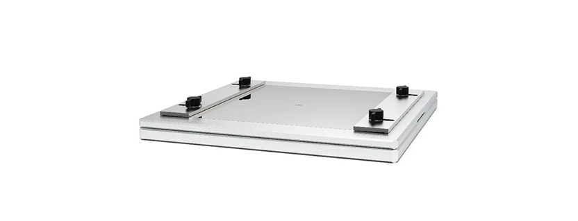
1.2 The Anatomy of a Fixture for Manual Solder Paste Application
The exploded view of the manual fixture utilized in applying the solder paste pattern to the PCB is shown in Figure 2. Guide pins are utilized to positively locate the top plate as well as the PCB adapter (pedestal) into the baseplate. Thumb screws and brackets (collectively referred to as “fasteners”) secure the stencil to the top plate, once it is aligned carefully using a microscope.

Figure 2: Exploded view of fixture assembly showing baseplate with guide pins, top plate, adapter (pedestal), PCB, and stencil/fasteners.
It is worth mentioning again that the purpose of the adapter (pedestal) is to ensure that the top surface of the PCB is flush with the plane at which the bottom surface of the stencil is secured. The fully assembled fixture, ready for solder paste application, appears as shown in Figure 3A. Figure 3B is a cutaway view illustrating the underlying PCB and adapter.


Figure 3A (left): Completely assembled fixture and 3B (right) cutaway view showing PCB resting on adapter (pedestal) covered by stencil.
1.3 Point Critical – Assembling the Fixture and Securing the Stencil
The following procedure is true of this style fixture, but may not apply to every fixture. One critical step is a prerequisite for any solder paste application, and that step is the lateral alignment of the stencil, which should always be done under a microscope for HK-series μCeramIQ™ components in the NM1812C-3 case style.
1. Begin by putting on latex gloves (or finger cots, at a minimum) to avoid depositing finger oils onto the fixture surfaces or the PCB itself.
2. Set the PCB adapter (pedestal) in place on the guide pins in the baseplate
3. Set the top plate in place (without the stencil) on its guide pins that are also anchored in the baseplate
4. Set the PCB (component side up) on top of its adapter in the opening left by the top plate. The PCB may jig itself into place using the top plate cavity, as shown, or may be further held in place by screws or guide pins themselves
5. Set the 0.003” thick stencil in place over the top of the PCB
6. Loosely install the fasteners that will ultimately hold the solder stencil in place. Be sure that the stencil can still be moved readily, in the x, y-plane (i.e., laterally)
7. Slide the entire fixture underneath a suitable microscope (10X-to-100X is more than sufficient)
8. Focusing on the apertures in the stencil, try to locate the input and output terminals of the HK-series μCeramIQ™ component footprint on the PCB by sliding the stencil laterally (note: this may require getting it close with the naked eye, then utilizing the microscope)
9. Once the input and output terminals have been located, as shown in the left-hand portion of Figure 4, continue to make very subtle adjustments to the stencil position until the apertures for these terminals are virtually concentric with the pads themselves, as shown on the right side of Figure 4
10. Carefully secure the stencil in place with the fasteners, making certain to compensate for any slight movement of the stencil seen under the microscope

Figure 4: Stencil-PCB aligned/positioned incorrectly (upper left), correctly (upper right), and also shown using a microscope (lower left and lower right).
1.4 Applying Solder Paste, Component Placement, and Reflow
11. With the fixture now fully assembled and correctly aligned, remove a sufficient amount of solder paste from the container using the spatula and apply it to the rubber blade of the squeegee (i.e., the amount of solder paste must be guaranteed to cover all stencil apertures. Significantly more than is required is shown in Figure 5.)
- Any solder paste stored in a refrigerated environment must be allowed to assume room temperature before being applied.
- The reason for guaranteeing 100% aperture coverage with the solder paste is that only one pass may be attempted with the squeegee, shown by the blue arrow in Figure 5. The applied solder paste must never be touched up or reworked
- If the solder paste application process or coverage is compromised in any way, the fixture, every tool, and the PCB must all be totally cleaned, and the process started again at Step 1
12. If the single pass with the squeegee was successful, set the squeegee aside and proceed to step 13

Figure 5: Fixture with stencil fastened in place during application of solder paste. The blue arrow signifies that only one squeegee stroke is made.
13. Do not unfasten the stencil; instead, lift the top plate/stencil/fasteners subassembly directly off the bottom plate in a vertical direction (along the axis of the guide pins) as shown in the top view of Figure 6
14. Inspect the application of the solder paste for filled apertures and uniformity of thickness.
- Avoid overfilling the apertures with excess solder paste that is too thick, as this tends to create short-circuits between the input/output and ground when reflowed.
- The bottom view of Figure 6 shows an excellent (passing) result.


Figure 6: Top plate/stencil lifted off vertically (upper), resulting in uniformly deposited solder paste (lower) (solder mask not shown for clarity).
15. With the solder paste now applied successfully, place the bottom plate/adapter/PCB subassembly under the microscope, and focus on the area delineated by the solder mask.
16. Pick the HK-series μCeramIQ™ component up using tweezers in the preferred direction, either lengthwise (as shown in the top view in Figure 7) or widthwise.
17. Gently lower the filter into place within the confines of the solder mask, as shown in the bottom view of Figure 7
- It is often helpful to lower the component until it hovers just slightly above the solder paste and, while well-aligned laterally, “drop” the component into place.
- While dropping the component may sound unusual, it avoids any slight motion present in the operator’s grip that may disturb the underlying solder at touch-down. A well-aligned component can then be “slid” perfectly into place by the operator using the side of the tweezers.
- At this point, some operators will impart ever-so-slight downward pressure to the component to compress the solder paste; others will leave well enough alone, knowing full well that the surface tension at reflow of the various solder menisci will tend to “pull” the filter to the board and often into finer lateral alignment.


Figure 7: HK-series μCeramIQ™ component being placed utilizing tweezers and with the aid of a microscope (upper). Properly-placed HK-series μCeramIQ™ component (lower).
18. With the component placed on the PCB, and necessary precautions being taken not to bump the assembly in the handling process, the operator can proceed to reflow
19. It is not just strongly suggested but virtually required that the reflow operation be achieved using a suitable 7-zone oven. While it is not entirely impossible to reflow a μCeramIQ™ component at this stage using a hot-air station or hot plate, the 7-zone oven exercises the control necessary to ensure excellent quality, both electrically and mechanically. The PCB can be placed in a tray or holder prior to entering the oven.
20. While preheating and soaking can take several minutes, the most critical (reflow) portion of the oven profile must have a peak temperature in the 235⁰C to 255⁰C range and a time at which the temperature exceeds 217⁰C in the 60-75 second range, and not exceeding 90 seconds. The zone temperatures below, combined with Mini-Circuits’ time profile, meet the aforementioned requirements.

1.5 The Payoff Pitch
Once the PCB assembly completes reflow, it is ready to be cooled, inspected, and tested. Inspection is a bit difficult, as the interfaces to the μCeramIQ™ component package are all underneath the part. X-ray is often required, and sometimes relied upon, but many times it is not utilized for small-quantity, individually-assembled runs of PCBs. The ground connection around the periphery can be a telltale sign of the quality of the soldering (see the finished part in Figure 8), and if there are no voids in this area, there are likely no voids underneath. However, bridges resulting from too much solder are inordinately difficult to detect.

Figure 8: HK-series μCeramIQ component after manual solder application, manual component placement, and 7-zone oven reflow
The high-performance HK-series of μCeramIQ™ components embodies disruptive technology. In particular, for the filter sub-line, these components exhibit 80 to 100 dB of rejection in a package as small as 1812. If not soldered properly, however, that rejection can be compromised. Follow the steps in this procedure and continue to enjoy the exceptional performance this disruptive technology has become known for.
Watch the tutorial video below:
Contact
Mini-Circuits
13 Neptune Avenue
Brooklyn, NY 11235
Phone: +1-718-934-4500
Email: sales@minicircuits.com
Web: www.minicircuits.com
Important Notice
This document is owned by Mini-Circuits and is protected by copyright, trademark and other intellectual property laws.
The information herein is provided by Mini-Circuits as an accommodation to our customers and may be used only to promote and accompany the purchase of Mini-Circuits’ parts. This guide may not be reproduced, modified, distributed, published, stored in an electronic database, or transmitted and the information contained herein may not be exploited in any form or by any means, without prior written permission from Mini-Circuits.
This guide is subject to change, qualifications, variations, adjustments or modifications without notice and may contain errors, omissions, inaccuracies, mistakes or deficiencies. Mini-Circuits assumes no responsibility for, and will have no liability on account of, any of the foregoing. Accordingly, this document should be used as a guideline only.
Courtesy of Mini-Circuits