The Anti-Parallel Series Pair Limiter Topology
The PIN Diode and the Anti-Parallel Configuration
The PIN diode itself was invented by Jun-ichi Nishizawa in 19501, just 18 days before R. N. Hall of General Electric. Hall would go on to propose the PIN diode as a rectifier in 19522, and a decade later the anti-parallel PIN diode limiter configuration had essentially become mainstream and was not presented as anything novel.
For more than 6 decades PIN diode limiters have served to enhance the robustness of RF receivers. The anti-parallel configuration is a very popular choice because its insertion loss, recovery time, power handling, flat leakage and frequency response characteristics can be traded off readily by choice of PIN diode. Even increasing the number of PIN diodes utilized in a limiter circuit can affect performance whether they are added in series or in subsequent stages altogether.
Mini-Circuits’ limiters come in a number of configurations and in surface mount, coaxial and plug-in case styles. Of particular note is the CLM-83-2W+. This surface mount limiter has a maximum RF input power of 2W and a frequency range that extends to 8.2 GHz in a package that is just 3mm x 3mm.
Since a great deal of literature is already available on limiter fundamentals3,4,5, this article shows the simulated performance of one specific PIN diode limiter configuration, two anti-parallel series pairs. Running an input power sweep in the time domain over 60 dB dynamic range yields an interesting set of results in both the time and frequency domains, and a description of the spectral content is provided. The article then cites an example of a component in which this limiter design configuration is utilized and a system for which that component finds a design application.
Anti-Parallel Series Pairs
Figure 1 reflects the chosen design topology by showing two anti-parallel series pairs of Rohm RN779D6 PIN diodes. These diodes were chosen because their simulation model was readily available and they are nearing EOL. The goal is to showcase a circuit comprised of two anti-parallel series pairs in significant detail in the time and frequency domains. This tried-and-true limiter topology and legacy PIN diode are all that is needed to perform good, representative circuit simulations.

Figure 1: Limiter configuration comprised of anti parallel RN779D PIN diode pairs simplified to show only the PIN diodes
Simulation Set-Up – Voltage, Time and Frequency
The goal is to execute an RF input power sweep in the time domain for 60 dB of dynamic range, from -20 to +40 dBm. In the time domain, this involves ramping up our sinusoidal CW RF input voltage generator Vin(t) from a peak voltage of 31.6 mV (-20 dBm power) to a peak voltage of 31.6V (+40 dBm power). Therefore, the simulated limiter output at the cathode of D2 will be the resultant voltage waveform Vout. Next, we select a convenient frequency of 100 MHz, which is nearly an order of magnitude within the capability of the PIN diode. And finally, with respect to simulation time, an easy way to both set up the simulation and to view it, is to allow the RF input source to ramp its power linearly over both the desired dynamic range and time. Consequently, the RF input power level is increased (swept) by 60 dB over 60 μs. This corresponds to a 1 dB change every 1 μs, also allowing a full 10 cycles of the RF input waveform for every dB of power change.
PIN Diode Limiter Simulation Results – Time Domain

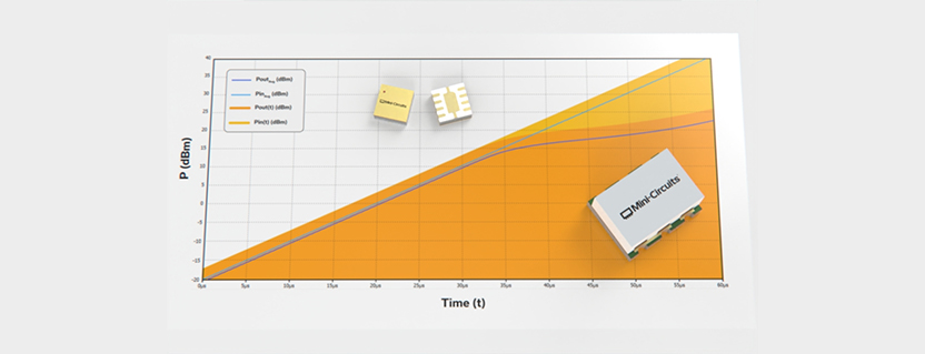
Figure 2: Time domain simulation results at 100 MHz for limiter comprised of two anti-parallel pairs of RN779D PIN diodes
The time domain simulation results utilizing the set-up described in the previous section are shown in Figure 2. The light orange section is the continuous, instantaneous RF input power waveform, computed from the sinusoidal RF input voltage squared as Pin(t) (dBm) = 10log{[Vin2sin2(ωt)/50]/.001}. Similarly, the dark orange section is the instantaneous RF output power waveform, computed from the voltage Vout(t) squared as Pout(t) (dBm) = 10log{[Vout(t)2/50]/.001}. Therefore, the light blue trace is the average RF input power and the dark blue curve the average RF output power. There are a few points to note. The knee of the RF output power curve occurs just below 15 dBm of RF input power. The point at which the limiter exhibits 1 dB of compression is just slightly above an RF input power of 15 dBm. For an RF input power level of +20 to +30 dBm, the limiter performs well, with leakage remaining relatively flat, ranging between 16 and 18 dBm.
A realistic upper bound on the maximum RF input power level for this PIN diode limiter is 1W. Anything above that will likely cause some or all of the smoke contained within the PIN diode intrinsic region to be released. At 1W (+30 dBm) RF input, the flat leakage of the limiter is approximately 18 dBm.
Frequency Domain Simulation Results – Small Signal
The PIN diode limiter output is quite linear when backed off from the onset of limiting (knee of the compression curve). In this linear region, we would expect signals with relatively modest PAPRs to pass undistorted through the limiter. In the case of a small signal sinusoidal CW waveform, the harmonic distortion at the limiter output should be negligible, and this should be manifest in the spectral plot for the output signal in the frequency domain. Figure 3 shows the RF output spectrum for a CW 100 MHz signal at an RF input power level that sweeps through -10 dBm.

For the simulation, the RF input power level was constrained to sweep between the 9 and the 11 μs points (-11 to -9 dBm) of the overall RF input power range. The RF output fundamental (100 MHz) is then normalized to 0 dB so that the harmonic levels can be read directly. An FFT is performed to achieve the frequency spectrum in Figure 3. As expected, the harmonic distortion is quite low, with both the 3rd and 5th harmonics below -40 dBc, and the 7th and higher-order harmonics below -50 dBc.
Compression Manifest in the Frequency Domain – Large Signal
Unlike the RF output spectrum when a small signal RF input (-10 dBm) is utilized, RF output spectra under high-level (large signal) RF input conditions exhibit significant distortion, rich in odd harmonics (recall that an ideal square wave is an infinite series of odd harmonics). Case in point, examine Figure 4, the RF output spectrum for an RF input level within the approximate +30 dBm range. Again, an FFT of the RF output spectrum was performed and the results normalized to 0 dB for the fundamental. The portion of the simulation utilized to achieve a large signal RF input was 49 to 51 μs, corresponding to +29 to +31 dBm.

Notice how the 3rd harmonic is slightly higher than -12 dBc, the 5th harmonic is between -16 and -17 dBc, and the remainder of the odd harmonics decline gradually with harmonic frequency. Rest assured that the PIN diodes of the limiter saturate on each half cycle of the sinusoidal RF input waveform, creating more of a square wave at the output of the limiter. The limiter is approximately 12 dB compressed at this point.
Where Limiters are Used – A Practical Example
A practical example of a limiter that is topologically related to, but far superior in performance to the circuit configuration studied in this article is the Mini-Circuits’ RLM-33H+. This limiter component can be found in a previous article Modernizing a Legacy 16-Way Receiver Multicoupler with Mini-Circuits Parts – Mini-Circuits Blog7 protecting a pair of PHA-11+ devices that are combined into a single surface mount MMIC package. This affords a great deal of protection, particularly in light of the fact that the predecessor design had no limiter whatsoever.
Reached the Limit
Simulated performance of the PIN diode limiter configuration consisting of two anti-parallel series pairs was examined in both the time and frequency domains. In the time domain, a continuous and simultaneous sweep of RF input power and time yielded a set of curves for the RF input and RF output power over a 60 dB dynamic range. The results showed an RF output compression curve and relatively flat leakage up to approximately 1W (+30 dBm), the assumed RF input power limit. Frequency domain plots were provided for small signal (-10 dBm) and large signal (+30 dBm) RF input power levels, and harmonic content examined to determine the level of distortion. An example is provided of a 16-way receiver multicoupler system in which a Mini-Circuits’ limiter component RLM-33H+ is utilized, which has the same type of design topology as that discussed in this article.
References
- Famed Inventor Seeks to Dispel Belief That Japanese Are Copiers, Not Innovators – Los Angeles Times
- Hall, R. N. (1952). “Power Rectifiers and Transistors.” Proceedings of the I.R.E., Vol. 40, Issue 11, pp. 1512-1518
- An Introduction to Limiters – Mini-Circuits Blog
- High Power Limiter Modules – Mini-Circuits Blog
- Frequently Asked Question About Limiters – Mini-Circuits Blog
- RN779DT146 : Diodes
- Modernizing a Legacy 16-Way Receiver Multicoupler with Mini-Circuits Parts – Mini-Circuits Blog
Get in touch for orders or any queries: sales@rfdesign.co.za / +27 21 555 8400
Courtesy of Mini-Circuits