
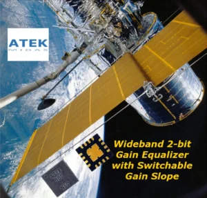
ATEK MIDAS Features Gain Equalizer with a Switchable Gain Slope that Balances Technical Performance with Circuit Complexity
ATEK MIDAS has extended its compound semiconductor design capability to include GaN/SiC process nodes at 0.15 µm gate length, complementing our existing GaAs PHEMT and HBT design flows. This addition enables us to address applications that require the higher breakdown voltage, higher power density, and better thermal performance that GaN provides relative to GaAs.
Why GaN?
Gallium nitride (GaN) on silicon carbide (SiC) substrates offers power density advantages of 5–10× over GaAs at equivalent gate periphery, making it the preferred technology for high-power amplifiers in L-band through Ka-band. Key applications include solid-state power amplifiers (SSPAs) for satellite uplink earth stations, active electronically scanned array (AESA) radar transmit/receive modules, electronic warfare jamming transmitters, and 5G mmWave base station power amplifiers.
ATEK MIDAS GaN Design Capability
ATEK MIDAS access qualified GaN/SiC foundry processes with proven RF device models and a history of successful tape-outs. ATEK MIDAS design team has experience in the specific challenges of GaN circuit design: thermal management at the transistor and layout level, bias sequencing and protection circuits, and reliability assessment in accordance with customer qualification requirements.
Engagement Model
GaN design engagements at ATEK MIDAS follow the standard IC productization flow — specification, architecture, design, verification, tape-out, and qualification — with foundry and packaging options selected to match each customer’s volume and performance requirements.
Get in touch for orders or any queries: sales@rfdesign.co.za / +27 21 555 8400
Courtesy of ATEK MIDAS